- 您现在的位置:买卖IC网 > Sheet目录3881 > PIC18F24K20-I/SO (Microchip Technology)IC PIC MCU FLASH 8KX16 28SOIC
PIC18F2XK20/4XK20
DS41297F-page 26
Advance Information
2009 Microchip Technology Inc.
4.3
Verify Configuration Bits
A configuration address may be read and output on
PGD via the 4-bit command, ‘1001’. Configuration data
is read and written in a byte-wise fashion, so it is not
necessary to merge two bytes into a word prior to a
compare. The result may then be immediately
compared to the appropriate configuration data in the
programmer’s
memory
for
verification.
Refer
to
Configuration Bits” for implementation details of
reading configuration data.
4.4
Read Data EEPROM Memory
Data EEPROM is accessed one byte at a time via an
Address Pointer (register pair EEADRH:EEADR) and a
data latch (EEDATA). Data EEPROM is read by loading
EEADRH:EEADR with the desired memory location
and initiating a memory read by appropriately configur-
ing the EECON1 register. The data will be loaded into
EEDATA, where it may be serially output on PGD via
the 4-bit command, ‘0010’ (Shift Out Data Holding
register). A delay of P6 must be introduced after the
falling edge of the 8th PGC of the operand to allow
PGD to transition from an input to an output. During this
time, PGC must be held low (see Figure 4-4).
The command sequence to read a single byte of data
is shown in Table 4-2.
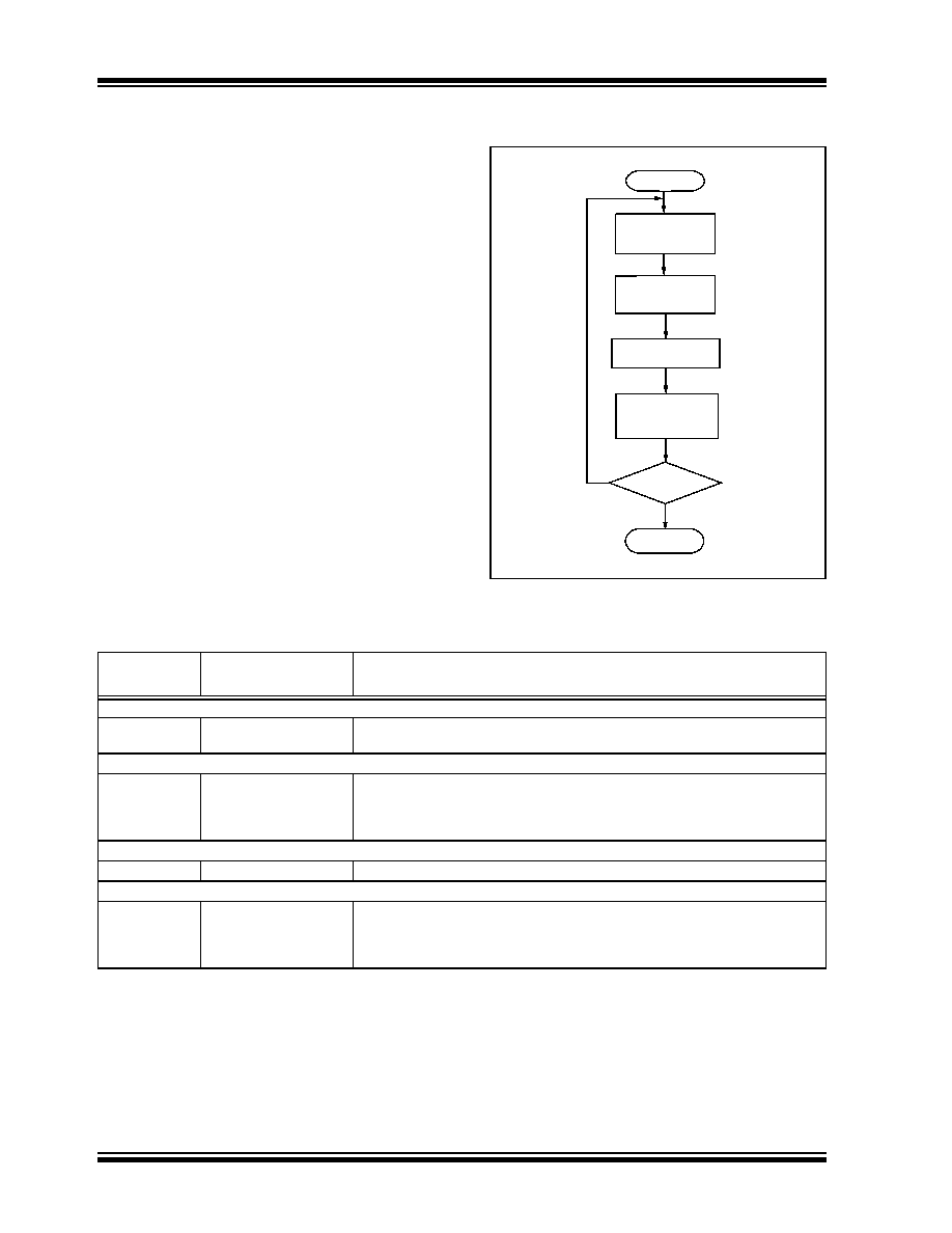
FIGURE 4-3:
READ DATA EEPROM
FLOW
TABLE 4-2:
READ DATA EEPROM MEMORY
Start
Set
Address
Read
Byte
Done
No
Yes
done?
Move to TABLAT
Shift Out Data
4-bit
Command
Data Payload
Core Instruction
Step 1: Direct access to data EEPROM.
0000
9E A6
9C A6
BCF
EECON1, EEPGD
BCF
EECON1, CFGS
Step 2: Set the data EEPROM Address Pointer.
0000
0E <Addr>
6E A9
OE <AddrH>
6E AA
MOVLW
<Addr>
MOVWF
EEADR
MOVLW
<AddrH>
MOVWF
EEADRH
Step 3: Initiate a memory read.
0000
80 A6
BSF
EECON1, RD
Step 4: Load data into the Serial Data Holding register.
0000
0010
50 A8
6E F5
00 00
<MSB><LSB>
MOVF
EEDATA, W, 0
MOVWF TABLAT
NOP
Shift Out Data
(1)
Note
1:
The <LSB> is undefined. The <MSB> is the data.
发布紧急采购,3分钟左右您将得到回复。
相关PDF资料
PIC18LF8585T-I/PT
IC PIC MCU FLASH 24KX16 80TQFP
XF2J-3024-11
CONN FPC 30POS 0.5MM SMT
PIC18LF6525T-I/PT
IC PIC MCU FLASH 24KX16 64TQFP
PIC18LF8621T-I/PT
IC PIC MCU FLASH 32KX16 80TQFP
PIC18F8620T-E/PT
IC PIC MCU FLASH 32KX16 80TQFP
PIC18F8720T-E/PT
IC PIC MCU FLASH 64KX16 80TQFP
PIC18F4439T-E/ML
IC PIC MCU FLASH 6KX16 44QFN
XF2J-2824-11
CONN FPC 28POS 0.5MM SMT
相关代理商/技术参数
PIC18F24K20-I/SP
功能描述:8位微控制器 -MCU 16KB Flash 768B RAM 25 I/O 8B RoHS:否 制造商:Silicon Labs 核心:8051 处理器系列:C8051F39x 数据总线宽度:8 bit 最大时钟频率:50 MHz 程序存储器大小:16 KB 数据 RAM 大小:1 KB 片上 ADC:Yes 工作电源电压:1.8 V to 3.6 V 工作温度范围:- 40 C to + 105 C 封装 / 箱体:QFN-20 安装风格:SMD/SMT
PIC18F24K20-I/SS
功能描述:8位微控制器 -MCU 16KB Flash 768B RAM 25 I/O 8B RoHS:否 制造商:Silicon Labs 核心:8051 处理器系列:C8051F39x 数据总线宽度:8 bit 最大时钟频率:50 MHz 程序存储器大小:16 KB 数据 RAM 大小:1 KB 片上 ADC:Yes 工作电源电压:1.8 V to 3.6 V 工作温度范围:- 40 C to + 105 C 封装 / 箱体:QFN-20 安装风格:SMD/SMT
PIC18F24K20T-I/ML
功能描述:8位微控制器 -MCU 16KB Flash 768B RAM 25 I/O 8B RoHS:否 制造商:Silicon Labs 核心:8051 处理器系列:C8051F39x 数据总线宽度:8 bit 最大时钟频率:50 MHz 程序存储器大小:16 KB 数据 RAM 大小:1 KB 片上 ADC:Yes 工作电源电压:1.8 V to 3.6 V 工作温度范围:- 40 C to + 105 C 封装 / 箱体:QFN-20 安装风格:SMD/SMT
PIC18F24K20T-I/SO
功能描述:8位微控制器 -MCU 16KB Flash 768B RAM 25 I/O 8B RoHS:否 制造商:Silicon Labs 核心:8051 处理器系列:C8051F39x 数据总线宽度:8 bit 最大时钟频率:50 MHz 程序存储器大小:16 KB 数据 RAM 大小:1 KB 片上 ADC:Yes 工作电源电压:1.8 V to 3.6 V 工作温度范围:- 40 C to + 105 C 封装 / 箱体:QFN-20 安装风格:SMD/SMT
PIC18F24K20T-I/SS
功能描述:8位微控制器 -MCU 16KB Flash 768B RAM 25 I/O 8B RoHS:否 制造商:Silicon Labs 核心:8051 处理器系列:C8051F39x 数据总线宽度:8 bit 最大时钟频率:50 MHz 程序存储器大小:16 KB 数据 RAM 大小:1 KB 片上 ADC:Yes 工作电源电压:1.8 V to 3.6 V 工作温度范围:- 40 C to + 105 C 封装 / 箱体:QFN-20 安装风格:SMD/SMT
PIC18F24K22-E/ML
功能描述:8位微控制器 -MCU 16KB Flash 768B RAM 8b FamilynanoWatt RoHS:否 制造商:Silicon Labs 核心:8051 处理器系列:C8051F39x 数据总线宽度:8 bit 最大时钟频率:50 MHz 程序存储器大小:16 KB 数据 RAM 大小:1 KB 片上 ADC:Yes 工作电源电压:1.8 V to 3.6 V 工作温度范围:- 40 C to + 105 C 封装 / 箱体:QFN-20 安装风格:SMD/SMT
PIC18F24K22-E/MV
功能描述:8位微控制器 -MCU 16KB Flash 768B RAM 8b FamilynanoWatt RoHS:否 制造商:Silicon Labs 核心:8051 处理器系列:C8051F39x 数据总线宽度:8 bit 最大时钟频率:50 MHz 程序存储器大小:16 KB 数据 RAM 大小:1 KB 片上 ADC:Yes 工作电源电压:1.8 V to 3.6 V 工作温度范围:- 40 C to + 105 C 封装 / 箱体:QFN-20 安装风格:SMD/SMT
PIC18F24K22-E/SO
功能描述:8位微控制器 -MCU 16KB Flash 768B RAM 8b FamilynanoWatt RoHS:否 制造商:Silicon Labs 核心:8051 处理器系列:C8051F39x 数据总线宽度:8 bit 最大时钟频率:50 MHz 程序存储器大小:16 KB 数据 RAM 大小:1 KB 片上 ADC:Yes 工作电源电压:1.8 V to 3.6 V 工作温度范围:- 40 C to + 105 C 封装 / 箱体:QFN-20 安装风格:SMD/SMT